Supported ESP32 Board Variants
IoT Carrier v0.1 is designed to support multiple ESP32 development boards through a common electrical interface and standardized pin headers. This approach allows different ESP32 variants to be installed on the same carrier PCB without hardware redesign while maintaining identical peripheral connectivity.
The platform currently supports the following development boards:
- NodeMCU-32S (ESP32-WROOM-32)
- ESP32-C3-DevKitM-1
- DEVKIT V1
Although the supported boards differ in architecture and hardware resources, all of them provide full compatibility with the analog (ADC) and digital (I²C) peripherals implemented on the IoT Carrier v0.1.
NodeMCU-32S
| Feature | Description |
|---|---|
| Module | ESP32-WROOM-32 |
| Processor | Dual-core Xtensa® LX6, up to 240MHz |
| Memory | 520KB SRAM, 4MB SPI Flash |
| Wireless | Wi-Fi 802.11 b/g/n (2.4GHz), Bluetooth v4.2 + BLE |
| Interfaces | UART, SPI, I²C, I²S, PWM, timers, GPIO |
| ADC/DAC | 12-bit SAR ADC (18 channels), 2x8-bit DAC |
| USB Programming | CP2102 USB-to-UART bridge |
| Logic Level | 3.3V CMOS |
| GPIO | 34 |
Pin-Out Diagram
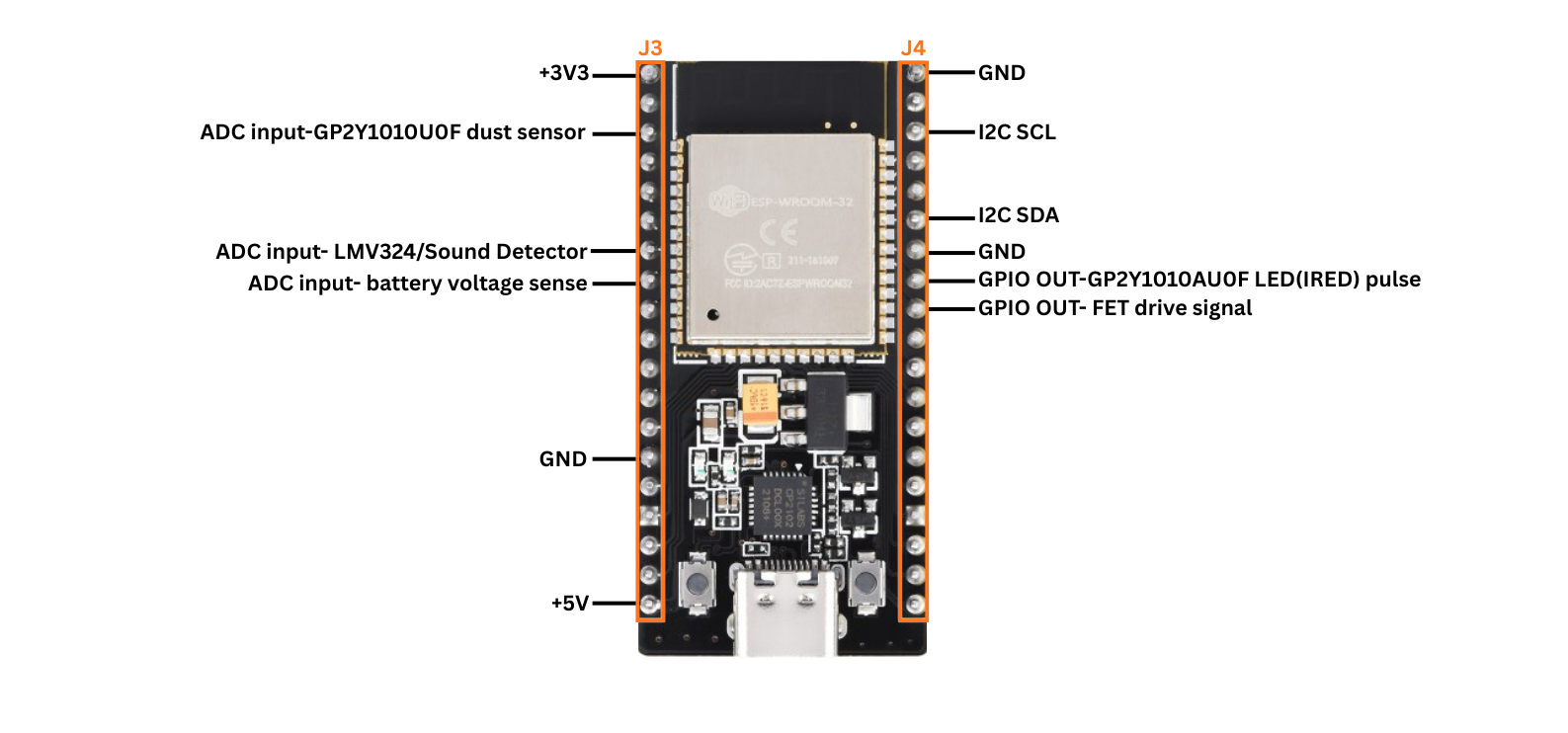
Figure 7. NodeMCU-32S pinout
| Pin Name | GPIO / Pin | Function in Prototype | PCB Header |
|---|---|---|---|
| SDA | GPIO21 | I²C data line | J4-06 |
| SCL | GPIO22 | I²C clock line | J4-03 |
| ADC-dust | GPIO36 (ADC1_CH0) | GP2Y1010AU0F analog output Vo | J3-03 |
| ADC-sound | GPIO32 (ADC1_CH4) | LMV324 | J3-07 |
| ADC-battery | GPIO33 (ADC1_CH5) | Battery voltage level detection | J3-08 |
| GPIO out | GPIO19 | GP2Y1010AU0F LED (IRED) | J4-08 |
| GPIO out | GPIO18 | FET signal | J4-09 |
| 3V3 | 3.3 V | Logic / sensor supply rail | J3-01 |
| 5V | 5.0 V | Dust sensor / Sound Detector supply | J3-19 |
| GND | GND | Common ground reference | J3-14; J4-01; J4-07 |
Table 2. NodeMCU-32S pin assignment used in the IoT Carrier v0.1 prototype.
C3-DevKitM-1
| Feature | Description |
|---|---|
| Module | ESP32-C3-MINI-1 |
| Processor | Single-core RISC-V, up to 160MHz |
| Memory | 400KB SRAM, 384KB ROM, integrated SPI Flash |
| Wireless | Wi-Fi 802.11 b/g/n (2.4 GHz), BLE 5.0 |
| Interfaces | UART, SPI, I²C, PWM, timers, GPIO |
| ADC/DAC | 12-bit SAR ADC (up to 6 channels), no DAC |
| USB Programming | Integrated USB Serial/JTAG controller |
| GPIO Count | 22 |
| Logic Level | 3.3 V CMOS |
Table 3. ESP32-C3-DevKitM-1 hardware features.
Pin-Out Diagram
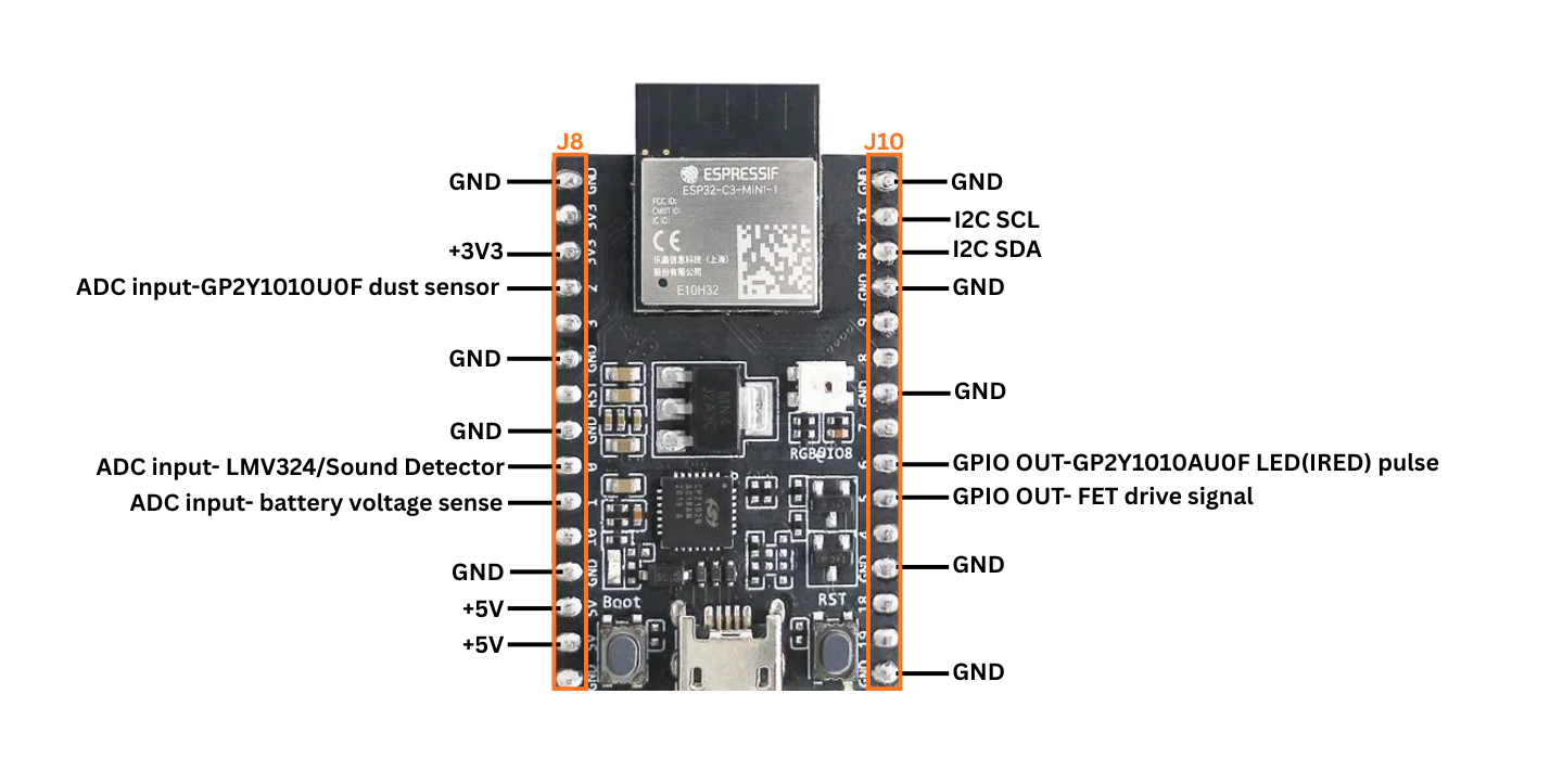
Figure 8. C3-DevKitM-1 pinout
DEVKIT V1
| Feature | Description |
|---|---|
| Module | ESP32-WROOM-32 |
| Processor | Dual-core Xtensa® LX6, up to 240MHz |
| Memory | 520KB SRAM, 4MB SPI Flash |
| Wireless | Wi-Fi 802.11 b/g/n (2.4 GHz), Bluetooth v4.2 + BLE |
| Interfaces | UART, SPI, I²C, I²S, PWM, timers, GPIO |
| ADC/DAC | 12-bit SAR ADC (18 channels), 2x8-bit DAC |
| USB Programming | CP2102 or CH340 USB-to-UART bridge |
| GPIO Count | 34 (with restrictions) |
| Logic Level | 3.3 V CMOS |
Table 4. DEVKIT V1 hardware features.
Pin-Out Diagram
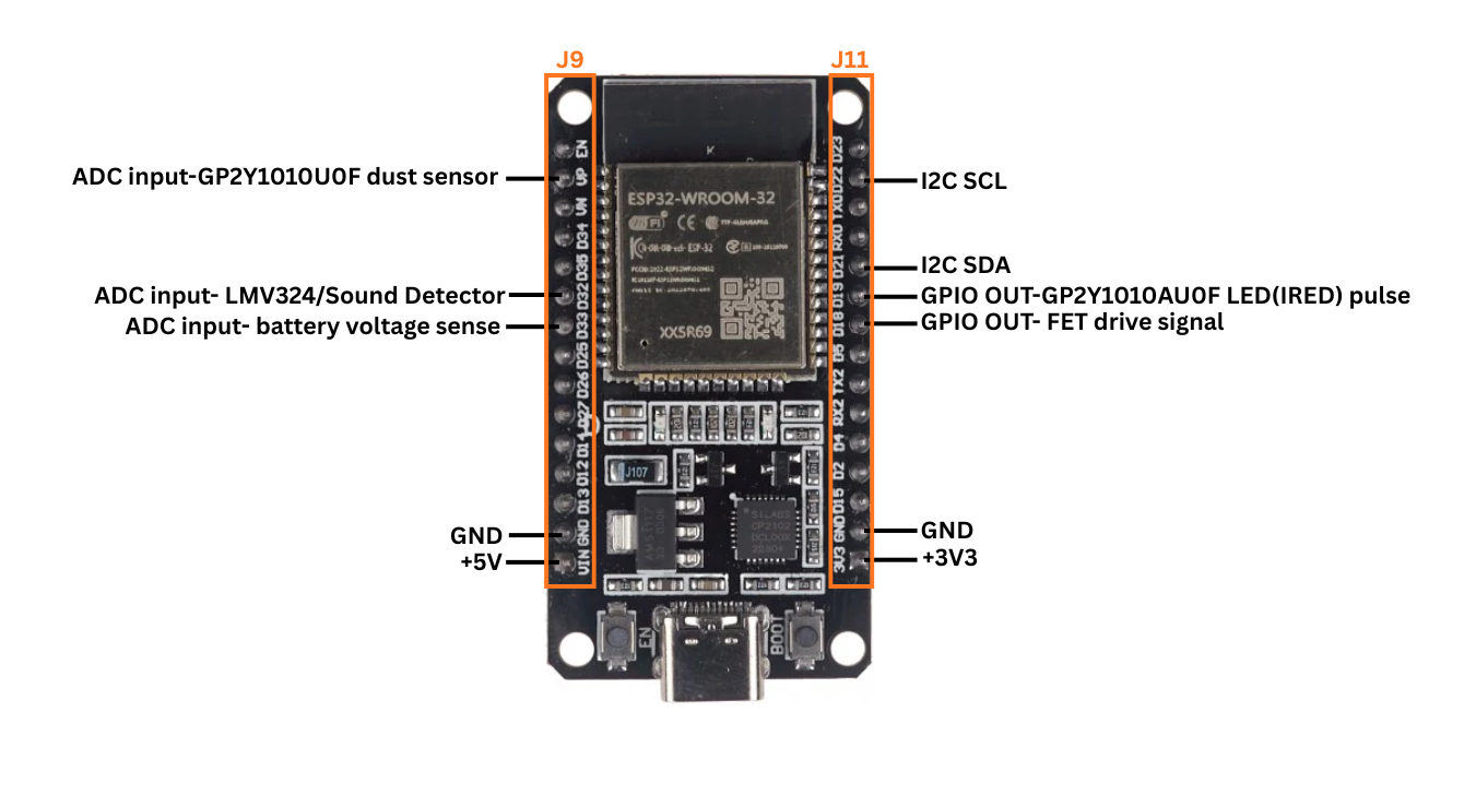
Figure 9. DEVKIT V1 pinout
| Pin Name | GPIO / Pin | Function in Prototype | PCB Header |
|---|---|---|---|
| SDA | GPIO21 | I²C data line | J11-05 |
| SCL | GPIO22 | I²C clock line | J11-02 |
| ADC-dust | GPIO36 (ADC1_CH0) | GP2Y1010AU0F analog output Vo | J9-02 |
| ADC-sound | GPIO32 (ADC1_CH4) | Sound Detector envelope output | J9-06 |
| ADC-battery | GPIO33 (ADC1_CH5) | Battery voltage sense | J9-07 |
| GPIO out | GPIO19 | GP2Y1010AU0F LED (IRED) pulse | J11-06 |
| GPIO out | GPIO18 | FET drive signal | J11-07 |
| 3V3 | 3.3 V | Logic / sensor supply rail | J11-15 |
| 5V | 5.0 V | Dust sensor / Sound Detector supply | J9-15 |
| GND | GND | Common ground reference | J9-14, J11-14 |
Table 5. DEVKIT V1 pin assignment used in the IoT Carrier v0.1 prototype.
Board Feature Comparison
| Feature | NodeMCU-32S | C3-DevKitM-1 | DEVKIT V1 |
|---|---|---|---|
| CPU | Dual-core Xtensa LX6, 240 MHz | Single-core RISC-V, 160 MHz | Dual-core Xtensa LX6, 240 MHz |
| Memory | 520 KB SRAM, 4 MB Flash | 400 KB SRAM, 384 KB ROM, SPI Flash | 520 KB SRAM, 4 MB Flash |
| Wireless | Wi-Fi + BT v4.2 + BLE | Wi-Fi + BLE 5.0 | Wi-Fi + BT v4.2 + BLE |
| USB Interface | CP2102 UART bridge | USB Serial/JTAG | CP2102 or CH340 UART bridge |
| GPIO Count | 34 | 22 | 34 |
| ADC/DAC | 12-bit ADC (18 ch), 2 DAC | 12-bit ADC (6 ch), no DAC | 12-bit ADC (18 ch), 2 DAC |
Table 6. Comparison of supported ESP32 development boards.